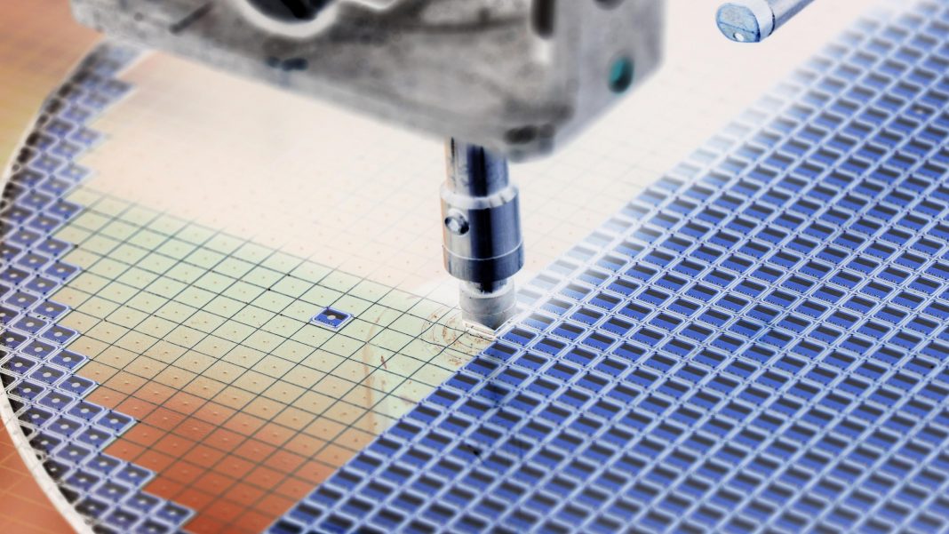
Enterprise Tech Imec Details Roadmaps For Advanced Logic And Memory Tom Coughlin Contributor Opinions expressed by Forbes Contributors are their own. May 24, 2022, 12:33am EDT | Share to Facebook Share to Twitter Share to Linkedin Silicon wafer in production getty Imec is a semiconductor and nanotechnology research center in Belgium. They recently made several announcements and a briefing on their developments. Imec works on health and many other areas but they are a leading developer of semiconductor technology, particularly on advanced lithography, working with ASML out of the Netherlands. They also do work on a number of memory technologies. Let’s look at some recent developments. Imec discussed a number of roadmaps. The figure below shows their vision of the development of wireless communication out to the end of the decade as we move into ever higher frequency communication. These higher frequencies require compound semiconductor (such as InP) devices connected with CMOS logic in a planar package with an RF interposer. imec 6G Roadmap IMEC Briefing Sri Samavedam spoke about imec’s logic technology evolution. The number of transistors is chip appears to be continuing Moore’s Law growth, with the Apple M1 Ultra having 114B transistors in March 2022. Although Moore’s law continues, single thread performance growth has slowed a lot and chip design costs continue to grow. This has driven the use of various domain specific processors. Important characteristics for future chips are dimensional scaling, new materials and device architectures and system technology co-optimization. The figure below is a version of imec’s lithographic roadmap. Current 2-7nm lithography semiconductors are using the first generation of extreme ultraviolet (EUV) lithographic equipment from ASML. Imec and ASML are working together on a new high numerical aperture hNA EUV machine in a laboratory in the Netherlands with a goal of bringing a hNA EUV into production by 2027 (much faster than the original ASML EUV machine). MORE FOR YOU The 5 Biggest Technology Trends In 2022 ‘Enthusiastic Entrepreneurs’: Pre-IPO Statements On Profitability Prove To Be Larger Than Real Life The 7 Biggest Artificial Intelligence (AI) Trends In 2022 imec Lithology Roadmap imec Briefing Sri also talked about BEOL scaling, optimizing resistance and capacitance, wafer backside power delivery and various 2 and 2.5D chiplet architectures, which imec called system technology co-optimization (STCO). There was also discussion of 3D chip system integration systems including CMOS imagers, HBM-DRAM stacks and high performance computing. The Apple M1 Ultra uses an embedded Si-bridge package. The image below shows an imec roadmap for 3D wafer connection integration. They also said that one of the big needs for 3D device design is EDA tools that enable such complex 3D designs. Approached to 3D chip interconnection imec Briefing Arnaud Furnemont spoke about storage and memory technology development at imec. Memory is facing demands for faster performance, lower cost and lower power consumption. The slide below developments in MRAM technology, which is finding growing opportunities especially in embedded devices. Arnaud also mentioned developments in 3D memories, which are moving from NAND to possible 3D DRAM and early research on 3D SRAM. MRAM memory developments imec Briefing He also spoke about DNA memory for long term storage and several concepts for liquid memory. There was also a lot of discussion around creating more sustainable semiconductor manufacturing. Lars Ake Ragnarsson pointed out that research shows that nearly 75% of a mobile device’s carbon footprint is due to its fabrication. Imec has been working on sustainable virtual fab as well as working with equipment and materials suppliers as well as foundry and IDM players to improve process and equipment and materials usage. Imec is a leading semiconductor and nanotechnology development organization. Imec roadmaps show lithography advances to a few angstrom features and enabling 3D integration. New memory technologies will combine with current memories to enable storage and processing the incoming tsunami of data. Follow me on Twitter or LinkedIn . Check out my website . Tom Coughlin Editorial Standards Print Reprints & Permissions
From: forbes
URL: https://www.forbes.com/sites/tomcoughlin/2022/05/24/imec-details-roadmaps-for-advanced-logic-and-memory/


