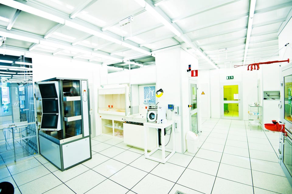
Enterprise Tech Semiconductor Equipment Spending Increases For Higher Density Logic And Memory Tom Coughlin Contributor Opinions expressed by Forbes Contributors are their own. New! Follow this author to improve your content experience. Got it! Jul 22, 2022, 12:51am EDT | New! Click on the conversation bubble to join the conversation Got it! Share to Facebook Share to Twitter Share to Linkedin Wide angle image of a cleanroom for fabrication of semiconductor devices getty SEMI, the leading international semiconductor trade organization held its Semicon conference in San Francisco in July.
SEMI predicts significant growth in semiconductor equipment demand in 2022 and leading into 2023 to meet demand for new applications and shortages for existing products, such as automobiles. We also look at some developments to make smaller featured semiconductors using EUV. SEMI released a press release from its Mid-Year Total Semiconductor Equipment Forecast during Semicon, about the state of semiconductor equipment spending and projections for 2023.
SEMI said that global sales of total semiconductor manufacturing equipment by original equipment manufacturers are forecast to reach a record $117. 5 billion in 2022, rising 14. 7% from the previous industry high of $102.
5 billion in 2021, and increase to $120. 8 billion in 2023. The figure below shows recent history and projections out to 2023 for semiconductor equipment sales.
Semiconductor Fab Equipment Forecast by Application SEMI Press Release Wafer fab equipment spending is projected to expand 15. 4% in 2022 to a new industry record of $101B in 2022 with a further 3. 2% increase projected in 2023 to $104.
3B. The figure below shows SEMI’s estimates and projections for equipment spending by semiconductor application. SEMI Semiconductor Process equipment Forecast SEMI Press Release MORE FOR YOU The 5 Biggest Technology Trends In 2022 ‘Enthusiastic Entrepreneurs’: Pre-IPO Statements On Profitability Prove To Be Larger Than Real Life The 7 Biggest Artificial Intelligence (AI) Trends In 2022 SEMI says that, “Driven by demand for both leading-edge and mature process nodes, the foundry and logic segments are expected to increase 20.
6% year-over-year to $55. 2 billion in 2022 and another 7. 9%, to $59.
5 billion, in 2023. The two segments account for more than half of total wafer fab equipment sales. ” The release goes on to say that, “Strong demand for memory and storage continues to contribute to DRAM and NAND equipment spending this year.
The DRAM equipment segment is leading the expansion in 2022 with expected growth of 8% to $17. 1 billion. The NAND equipment market is projected to grow 6.
8% to $21. 1 billion this year. DRAM and NAND equipment expenditures are expected to slip 7.
7% and 2. 4%, respectively, in 2023. ” Taiwan, China and Korea are the largest equipment buyers in 2022 with Taiwan expected to be the leading purchaser, followed by China and Korea.
Making smaller features has been a continuous driver for higher density semiconductor devices since the introduction of integrated circuits. Sessions at the 2022 Semicon explored how lithographic shrinks and other approaches, such as heterogeneous integration with 3D structures and chiplets, will allow continued increases in device density and functionality. During Semicon Lam Research announced a collaboration with leading chemical suppliers, Entegris and Gelest (a Mitsubishi Chemical Group company), to create precursor chemicals for Lam’s dry photoresist technology for extreme ultraviolet (EUV) lithography.
EUV, particularly the next generation of high numerical aperture (NA) EUV, is a key technology to drive semiconductor scaling, enabling features smaller than 1nm in the next few years. In a talk by David Fried, VP from Lam, showed that dry (composed of small metalorganic units) versus wet resists can provide higher resolution, a wider process window and higher purity. Dry resists for the same radiation dose, shows less line collapse and thus generation of defects.
In addition, dry resist use results in a 5-10X reduction in waste and cost and a 2X reduction in the power required per wafer pass. Michael Lercel, from ASML, said that high numerical aperture (0. 33 NA) is now in production for logic and DRAM as shown below.
The move to EUV reduces the extra process time and waste from multiple patterning to achieve finer features. High Numerical Aperture EUV in Production Semicon Presentation by ASML The image shows ASML’s EUV product roadmap and gives an idea of the size of the next generation EUV lithography equipment. ASML’s EUV Product Roadmap Semicon ASML Presentation SEMI predicted robust semiconductor equipment demand in 2022 and 2023 to meet demand and reduce shortages for critical components.
EUV developments at LAM, ASML will drive semiconductor features sizes below 3nm. Chiplets, 3D die stacks and the move to heterogenous integration will help drive denser and more functional semiconductor devices. Follow me on Twitter or LinkedIn .
Check out my website . Tom Coughlin Editorial Standards Print Reprints & Permissions.
From: forbes
URL: https://www.forbes.com/sites/tomcoughlin/2022/07/22/semiconductor-equipment-spending-increases-for-higher-density-logic-and-memory/


